by Shigetoshi Sugawa, Rihito Kuroda, Tohru Takeda, Fan Shao, Ken Miyauchi & Yasuhisa Tochigi
Graduate School of Engineering, Tohoku University 6-6-11-811, Aza-Aoba, Aramaki, Aoba-ku, Sendai, Miyagi, Japan 980-8579
ABSTRACT
In this work, a 20 Mfps global shutter CMOS image sensor with improved sensitivity and power consumption is demonstrated. Due to the process technology development and the improvement of single readout circuitry with decreased supply voltage, the fill factor, the conversion gain and the readout gain were all improved from the previous chip and eight times higher light sensitivity and 50% decrease of power consumption were achieved simultaneously. The impact of the performance improvements was confirmed to be significant based on the captured images of UHS phenomena.
INTRODUCTION
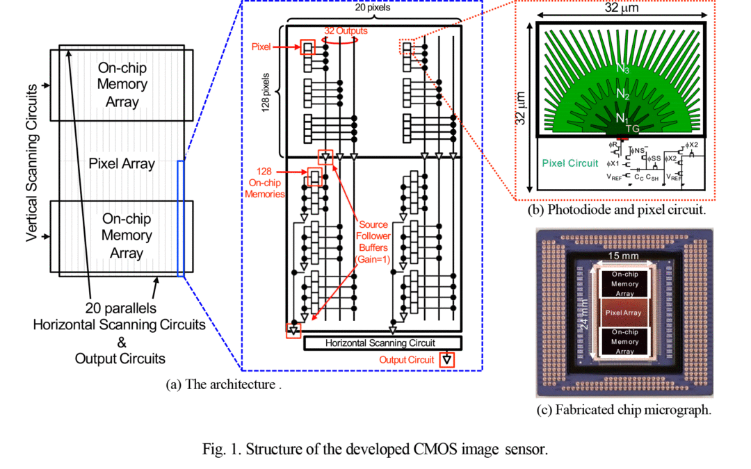
Ultra high-speed (UHS) imaging technologies are now being utilized in various scientific and engineering fields to reveal and analyze what has not been seen before. We have developed architecture for global shutter UHS CMOS image sensor with multiple onchip analog memories per pixel. The previously developed UHS CMOS image sensor has simultaneously achieved 10 Mfps, 10 Kpixels, 128 frames. In UHS imaging, sensitivity and power consumption are the major stumbling blocks to be overcome in order to improve the sensor performance to the next level. In this work, a newly developed UHS CMOS image sensor is demonstrated that achieves eight time higher sensitivity and 50% power consumption reduction simultaneously.